0.39-Inch 1080p Micro OLED EVFs: From Bench Prototype to Volume Tooling
Moving a 0.39-inch 1920x1080 Micro OLED panel from a dev board into a camera viewfinder is mostly a mechanical, optical and test problem, not a firmware one. The image itself does not change: it is still a 5644 PPI active-matrix OLED with MIPI and I2C interfaces, 16.7 million colours and a temperature rating that starts at -40 C. What changes is the flex, the mounting datum, the eyepiece stack, the connector retention and the test fixture that has to prove every assembled unit still works. The engineering sequence that decides whether the product ships on schedule is tooling and qualification, so define it before the first mechanical drawing is released. Own the stack end to end, and write down which interface each party is responsible for.
Key takeaways
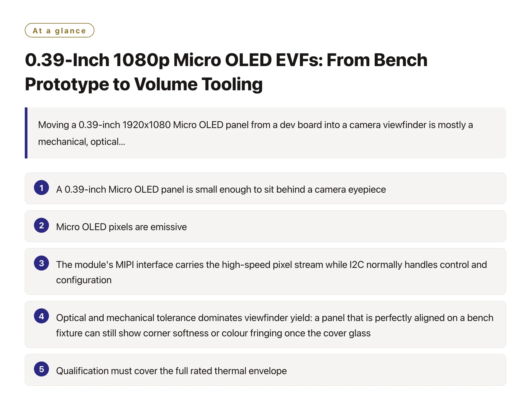
- A 0.39-inch Micro OLED panel is small enough to sit behind a camera eyepiece, and at 1920x1080 with 5644 PPI its pixel pitch is under five micrometres, so the practical limit on image quality is the eyepiece optics and the alignment of the panel to the optical axis rather than the panel itself; pixel density is conventionally expressed as pixels per inch along the panel. [3]
- Micro OLED pixels are emissive, so there is no backlight to heat the eyepiece assembly or to leak around the frame, but the same property means every defect in the emitting layer is visible rather than softened by a diffuser.
- The module's MIPI interface carries the high-speed pixel stream while I2C normally handles control and configuration, and the two have quite different signal-integrity and routing requirements even when they share one flexible cable.
- Optical and mechanical tolerance dominates viewfinder yield: a panel that is perfectly aligned on a bench fixture can still show corner softness or colour fringing once the cover glass, eyepiece element and housing are assembled, so alignment has to be specified as a measurable criterion rather than as a best effort.
- Qualification must cover the full rated thermal envelope, including the -40 C low end of the module's extreme-temperature rating, and it must add the local heating that your own electronics contribute inside the housing.
Development boards are forgiving. A flexible cable a few centimetres long, a socketed connector and a bench supply will happily drive a 0.39-inch panel at 1920x1080, and most engineers get a stable image on the first afternoon. The difficulty starts when that panel has to survive a camera body: a shorter and thinner flex with tighter bend radii, a connector that does not creep under vibration, and an eyepiece assembly whose optical axis has to line up with an active area only a few millimetres across.
Viewfinder products also invert the usual display priorities. The user looks through a magnifying eyepiece at very high angular resolution, so the acceptance criteria become focus uniformity across the field, colour uniformity, the absence of visible pixel structure, latency between the sensor and the eye, and how the image behaves when the diopter is adjusted. Because the image is magnified, a defect that would be invisible on a phone screen can be obvious here, and a defect that is obvious on a bench may disappear once the final optics are fitted.
This article walks through the transition from prototype to volume for a 1920x1080 Micro OLED viewfinder module: what to freeze first, how to treat the MIPI and I2C links as production interfaces, what the tooling and qualification sequence should contain, and which OEM and ODM questions are worth settling before anyone cuts metal.
Why the dev-board setup stops being representative
A development board hides three problems at once. It provides a generous flex with wide conductor spacing, plenty of clearance around the panel, and a connector that is never cycled more than a few dozen times. A camera does the opposite: the flex is folded into a few millimetres of space, the connector may be mated once in the factory, and the whole assembly is expected to hold alignment through drops, temperature cycling and years of use.
The panel itself is a 0.39-inch active-matrix Micro OLED with 1920x1080 resolution, 5644 PPI, 16.7 million colours and both MIPI and I2C interfaces. None of that changes on the way to volume, which is exactly the point: the electrical interface you validated on the bench is the right one, so the remaining risk lives in the mechanical and optical interface around it. Budget your engineering effort accordingly.
Write the stack up as a list. Emitter, cover glass, eyepiece elements, field stop, housing, adhesive, seal. Every entry has a tolerance and a coefficient of thermal expansion, and the sum of those tolerances decides whether the pixel grid stays sharp at the corners of the field after the housing warms up. If a layer cannot be named in that list, the design is not finished.
The cheapest time to find a stack-up error is on paper, before the flex artwork exists.
Bench assumptions versus volume requirements
| Subsystem | Bench prototype | Volume requirement | How it shows up when ignored |
|---|---|---|---|
| Display data link | Long flex on a dev board with a generous ground plane | Short controlled-impedance flex matched to the panel connector | Intermittent line errors that appear only at certain temperatures |
| Control channel | Jumper wires to a host header | Shared addressed bus with defined pull-ups and a documented address map | Bus lockups during bring-up that get blamed on the panel |
| Mechanical mount | Double-sided tape or a printed bracket | Datum features plus a bonded or clamped mount with a defined alignment method | Corner softness as the panel tilts inside the eyepiece |
| Eyepiece optics | One lens held by hand | Coated elements at fixed spacing with a repeatable focus process | Focus drift and colour fringing that appear only on assembled units |
| Test coverage | Eyes and a test pattern | Fixture with fixed patterns, current measurement and an alignment check | Escape of units with defects the customer notices immediately |
Treating the MIPI and I2C links as production interfaces
MIPI DSI is a high-speed serial display interface standardised by the MIPI Alliance, and it exists precisely for dense small panels: it moves the pixel stream over a handful of differential lanes instead of a wide parallel bus, which keeps the flex narrow enough to fold into a camera body. [1] What that buys you in board area it takes back in discipline, because a differential link is only as good as its reference plane and its length matching.
I2C is a multi-drop addressed serial bus, so several devices can share the same two wires provided their addresses do not collide. [2] That makes it a natural control channel for the panel in a viewfinder, but it also means the panel is sharing a bus with an image sensor, an ambient-light sensor, a gyroscope and whatever else the product needs. Draw the address map before layout, because an address collision discovered during board bring-up costs a re-spin.
Treat the panel's initialisation sequence as part of your firmware image rather than as an appendix to a datasheet. Record the exact command order, the delays between commands, and the state of the interface before and after reset, then keep that sequence in version control so a panel revision can be diffed against the one you qualified. Very few production display problems are solved by guessing at a register value on a bench at two in the morning.
Signal integrity on the flex deserves measurements instead of intuition. Check the differential impedance, the continuity of the reference plane under the connector, the stub length where the traces fan out to the pads, and the behaviour of the link across the full temperature range. Choose the module variant and the flex length together: a panel such as the 1920x1080 Micro OLED display with MIPI interface is delivered with its interface routed to a defined connector footprint, and the flex you design has to match both the impedance and the pin order without a re-spin, so agree the mechanical drawing before the first flexible circuit is ordered.
A tooling and qualification sequence that survives production
- Freeze the optical stack before the mechanical drawing. Fix panel position, eyepiece spacing and cover glass thickness first, because every later tolerance stacks on those three numbers. Releasing a housing drawing before the optics are frozen is the most common cause of a second tooling round.
- Build a flex and connector coupon, not a product. A small board carrying the same connector, the same stack-up and the same bend radius lets you test mating force, insertion loss and thermal cycling without committing to production tooling.
- Characterise the initialisation sequence across samples. Run the panel setup on units from more than one production lot and compare the results. If the picture shifts measurably between lots, the firmware needs a calibration step rather than a fixed table.
- Exercise the cold end of the temperature range. Because the module is rated for extreme temperatures with a low end of -40 C, cold start, flex stiffness and connector contact resistance all belong in the first qualification cycle, together with the local heating your own electronics add inside the housing.
- Design the production test fixture alongside the assembly. Decide what is checked on every unit and what is sampled per lot: test patterns for stuck or dead pixels, supply current, alignment through the eyepiece, and a latency measurement if autofocus or shutter feel depends on it.
- Agree the change-control and supply story. Confirm how a panel revision is notified, what triggers re-qualification, and which items such as the flex, cover glass or eyepiece can be second-sourced. A silent display change halfway through a programme is expensive to absorb.
Tooling is where a viewfinder programme quietly becomes expensive. The cover glass, the eyepiece mouldings, the flex and the test fixture are all custom, and each has a lead time that starts when the drawing is released. Every decision that lets you keep one of those items standard, such as using a module with a defined connector footprint or machining the first housing instead of moulding it, buys schedule back without touching image quality.
OEM and ODM questions worth settling before tooling
A display module can be customised along several axes, and the useful exercise is to sort the requests into those that change the panel and those that change only the assembly around it. Flex length and exit direction, connector type and pin assignment, cover glass outline and coating, mounting datums and the incoming inspection specification all sit in the second group and are usually quick to agree. Resolution, colour behaviour and interface type sit in the first group and are fixed by the panel you selected.
Compliance paperwork belongs in the same conversation as the mechanical drawing. RoHS restricts the use of hazardous substances such as lead, mercury and cadmium in electrical and electronic equipment, and a camera product will also need declarations covering adhesives, coatings and the flexible circuit. [4] Ask early which declarations ship with the part and which have to be produced specifically for your assembly, because the answer changes the release schedule.
What to ask about testing and traceability
Ask what is inspected on every unit and what is sampled per lot, and in what environment those measurements are taken, since a room-temperature check says little about a camera used outdoors in winter. Request the lot code on the label or in a readable register, so a field failure can be traced back to a build window rather than to a whole programme. If the supplier offers a report, agree its format now so that it can be parsed rather than retyped.
How to specify customisation without over-specifying it
Over-specified customisation is costly in two ways: it adds tooling that has to be amortised, and it removes the supplier's freedom to use standard parts and processes. Give the performance requirement instead of the construction, for example an alignment tolerance, a transmission figure, a bend radius and a temperature envelope, and let the supplier propose how to meet it. Then qualify the proposal against your own fixture rather than against a drawing.
Sources
Frequently asked questions
Can a 0.39-inch 1920x1080 Micro OLED panel be used in a camera electronic viewfinder?
Yes, and that is one of the main applications for this size class. At 5644 PPI the pixel pitch is small enough that a magnifying eyepiece produces a smooth image without visible pixel structure, and because the pixels are emissive there is no backlight adding heat next to the eyepiece. The remaining work is optical alignment and a housing that holds it across temperature.
Do I need both MIPI and I2C, or can I use just one interface?
The module supports both, and in a viewfinder they normally do different jobs: MIPI carries the high-speed pixel stream while I2C handles control and configuration. Some hosts push configuration over the same high-speed link, but keeping it on a separate low-speed bus makes bring-up and field diagnostics considerably easier. Decide this before the flex is routed, because the routing requirements differ.
What temperature range should the qualification plan cover?
Start from the module's rated range, which the supplier specifies from a low end of -40 C, and confirm the upper limit from the current datasheet rather than assuming it matches another part in the family. Then add the temperature rise caused by your own electronics, because the panel experiences the ambient inside the housing and not the outside air. Cold start deserves a separate test, since flex stiffness and connector contact resistance both change at low temperature.
How do I avoid a second tooling round on an EVF module?
Freeze the optical stack and the panel position before any housing drawing is released, and validate the flex, connector and alignment on a coupon rather than on production parts. Obtain the panel's mechanical drawing, the connector footprint and the initialisation sequence in writing, and put the alignment acceptance criterion into the drawing as a measurable number with an owner. Most second rounds come from a tolerance that nobody was assigned to control.